PN-Junction Diode:
A PN-junction diode is a basic semiconductor device in semiconductor electronics that is used in a wide variety of fields. A fundamental semiconductor device is a PN-junction diode. Either an ion implantation technique or the diffusion method is used to create a P-type crystal over the N-type crystal. The final crystal that is produced in this way is regarded as a single crystal, and the assembly is known as a PN-junction diode or crystal diode. A junction is a surface where P- and N-type crystals come into contact. While electrons predominate in the N-type section, holes are the predominant charge carriers in the P-type section.
The high concentration of different charge carriers in the two regions leads to hole diffusion from the P-region into the N-region and electron diffusion from the N-region into the P-region. When an electron and a hole come into contact, they cancel each other out in both situations, leaving a thin layer near the junction devoid of charge carriers. In Figure 9.2.01, the depletion layer is depicted. The depletion layer is approximately 10-6 m thick.
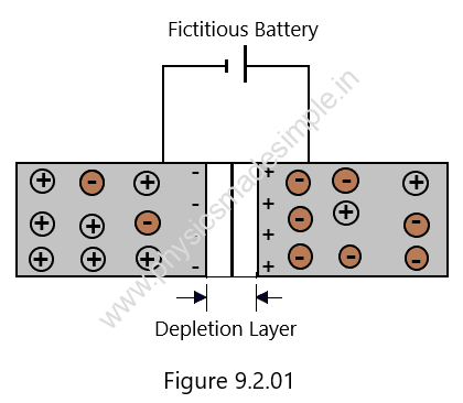
The two parts of the PN-junction diode are no longer neutral because of the diffusion of holes and electrons. The N-section of the junction diode is made positive, while the p-section becomes somewhat negative. The negative pole of a hypothetical battery seems to be connected to the P-region and the positive pole to the N-region when it is connected across the junction. The barrier potential is the differential in the potential that forms across the junction as a result of majority charge carrier diffusion. However, the value of the potential barrier depends on the doping concentration of the semiconductor crystal.
It may be pointed out that across the junction, a very large electric field is set up due to potential differences developed across it. Taking the width of the depletion layer of a silicon junction diode as 10-6 m and a potential difference of 0.7 V set up across it, the strength of the electric field is of the order of
E = 0.7/10-6 = 7 x 10⁵ V m-1.
Biasing of a PN-junction diode:
The biasing of a PN-junction diode means in what way it is connected to an external source of steady current (dc current). Accordingly, there are two types of bias.
Forward Bias:
The PN-junction diode is said to be forward-biased when an external dc source is connected to it, with its P-section connected to the positive pole of the battery and the N-section to the negative pole, as shown in Figure 9.2.02.

The PN-Junction Diode‘s mechanism: When the PN-Junction diode is forward-biased, the positive pole of the battery repels positive holes in the P-region away from the PN-Junction diode. The negative pole of the battery is simultaneously pulling the negative electrons in the N-section away from the junction. The artificial battery voltage (0.3 V to 0.7 V) created across the junction, however, opposes the passage of electrons and holes across it. Just before the PN junction, the potential barrier is crossed by the applied potential, which causes electrons and holes to merge and stop existing as mobile charge carriers.
A covalent bond breaks in the P-section close to the battery’s positive pole for each electron-hole pair that occurs there. The electron is taken out of the hole by the positive terminal, and an electron is created. The hole appears to be moving toward the junction. On the other hand, as soon as the covalent link breaks, creating a hole in the P-section, an electron is released from the battery’s negative terminal into the N-section to replace the electron lost when a hole and an electron combine at the junction.
As they approach the junction, these electrons are once again neutralized when they come into contact with the fresh holes flowing in from the left. As a result, the junction experiences a forward current that is relatively substantial in size. The electron drives the current in the external circuit, which travels from the battery’s negative terminal to its positive terminal via a PN-junction diode.
As was said before, the applied dc voltage opposes the fake battery formed across the PN-Junction Diode during the forward bias. The potential drop across the junction increases as a result, which in turn increases the diffusion of holes and electrons across the junction. The PN-Junction diode has low resistance during the forward bias because it thins the depletion layer.
Reverse Bias:
The PN-junction diode is said to be reverse-biased when an external DC source is connected to it, with the P-section connected to the negative pole of the battery and the N-section to the positive pole, as shown in Figure 9.2.03.
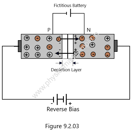
The PN-Junction Diode works as follows: When the PN-Junction diode is reverse biased, the P-section’s holes (majority carriers) become attracted to the battery’s negative terminal and travel away from the junction. At the same time, the N-section’s electrons (the majority carriers) are drawn to the positive terminal and depart from the function. There is essentially no current flow because there are so few holes and electrons (minority carriers) in the area of the junction.
However, a modest current (a few microamperes) still flows because of thermally produced electron-hole pairs in both the P and N-regions. Because of the typical thermal energy of the crystal molecules, certain covalent bonds inevitably break. In the P-region, electrons released during this process go to the left across the junction, whereas holes created in the N-region move to the right beneath the battery’s electric field. The minority carriers retain a little electron-hole combination current known as reverse current as a result.
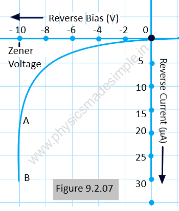
The reverse current climbs abruptly to a pretty high value when the reverse bias is set extremely high, causing all the covalent bonds close to the junction to shatter and a significant number of electron-hole pairs to be freed. The reverse breakdown voltage, also referred to as the Zener voltage, is the greatest reverse potential difference that a diode can withstand without breaking down. For silicon, it is higher than for germanium. Its value can range from 1 or 2 volts to several hundred volts and is dependent on the density of impurity atoms.
It should be noted that the applied DC voltage helps the fictional battery form across the junction during the reverse bias. The junction’s capacity to disperse holes and electrons decreases as a result of the increased potential drop across the junction. When the bias is reversed, it thickens the depletion layer and increases the junction diode’s resistance. It is important to remember that the potential barrier favors the reverse current while opposing the forward current.
Characteristics of the PN-Junction Diode:
Forward Bias Characteristics:
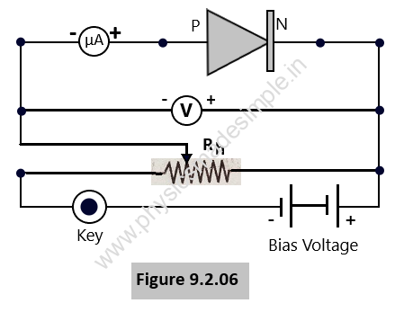
Forward Bias connections of a PN-Junction Diode are made as per the circuit diagram shown in Figure 9.2.06, where the positive terminal of the battery is connected to the P-section and the negative terminal of the battery is connected to the N-section of the PN-Junction Diode.
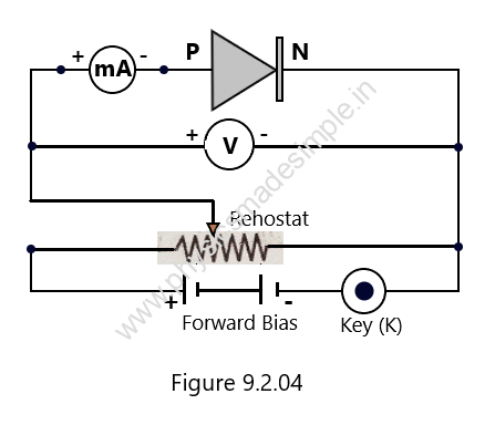
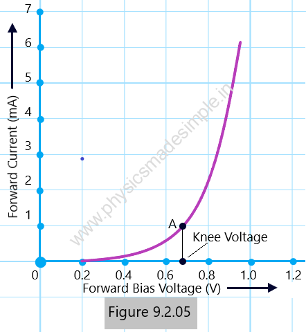
The forward current is noted corresponding to the different values of forward bias voltages applied, and the graph is drawn, which is similar to that shown in Figure 9.2.05.
At first, practically no current flows through the junction diode because of the low supplied forward bias voltage. A germanium PN junction’s potential barrier opposes the applied voltage by about 0.3 V and 0.7 V, respectively, depending on the kind of junction. In order to prevent the applied forward bias voltage from exceeding the potential barrier voltage, a tiny forward current flows.
Figure 9.2.05.’s segment OA of the graph between forward bias voltage and forward current serves as its representation. The forward current rises virtually linearly as soon as the forward bias exceeds the potential barrier. Point A in the forward characteristics corresponds to the potential barrier that appears like a knee, and the forward voltage corresponding to knee point A is called knee voltage.
The current grows linearly and quickly above the new voltage when a PN-junction diode is forward-biased, but it changes very slowly below the knee voltage as the forward bias is increased. Furthermore, the depletion layer thins when the PN-Junction diode is forward-biased. The fictional battery that has been generated across the junction is opposed due to the polarity of the external DC source, which is the cause. The defining layer becomes thin as a result of the potential drop across the junction being reduced. During forward bias, it causes the junction diode’s low resistance.
Reverse Bias Characteristics:
The PN-junction diode is said to have the reverse bias if the P-section is connected to the battery’s negative terminal and the N-section to its positive terminal, as shown in Figure 9.2.06. A microammeter is used to measure the tiny current that flows during the reverse bias because, when the P-N Junction diode is reverse-biased, the current flow is caused by a minority of charge carriers.
The minority carriers must cross the PN junction despite the reverse bias’s opposition to the majority carriers. Therefore, by providing a reverse bias to the PN Junction, a current of approximately 1 to 2 microamperes is obtained. Up until the Zener voltage is achieved, it is nearly steady before rapidly increasing, as illustrated in Figure 9.2.07
The depletion layer thickens when the PN Junction is reverse-biased. It is because, in this instance, the fake battery is supported by an external DC source. The increasing thickness of the depletion layer causes an increase in the potential drop across the junction and makes the depletion layer appear thick. Under conditions of reverse bias, the PN junction has high resistance.
Dynamic Resistance:
The PN-Junction Diode is a nonlinear device and does not conform to Ohm’s law because both the forward bias and reverse bias characteristics of the PN-Junction Diode have knees.
The dynamic resistance of a PN-Junction Diode is defined as the ratio of small changes in bias voltage to the small changes in the current produced.
It is represented by Rd, is also called the AC resistance of the PN-Junction Diode and given by
Rd = (dV/dI)
Where dV and dI are the respective changes in bias voltage and the corresponding change in current. The region of the VI-characteristic curve, where the dynamic resistance of a PN-Junction Diode is almost independent of the applied bias voltage, is known as the linear region of the junction diode.
Applications of PN-Junction Diodes:
PN-Junction Diode as rectifier:
A rectifier is an electronic device that converts an alternating current into a unidirectional pulsating current is called a rectifier.
According to research on junction diode properties, the device offers a high-resistance path when reverse-biased and a low-resistance path when forward-biased. The junction diode can function as a rectifier thanks to this property. The junction diode receives opposing types of bias from the two half cycles of alternating input emf. The junction diode will become reverse-biased during the second half cycle if the first half cycle causes it to become forward-biased, and vice versa. In other words, the junction diode will conduct only during the alternating half cycles that bias it in the forward direction when an alternating EMF signal is placed across it.
Half-wave rectifier:
A rectifier that rectifies only one-half of each input AC cycle, is called a wave rectifier.
Principle:
It is based on the principle of the valve action of a PN-junction diode. It will be conducted only when it is forward-biased. That means a PN-Junction diode offers no resistance path when it is forward-biased and high resistance when it is reverse-biased. When AC input is applied to the junction diode, it gets forward-biased during the first half cycle and reverse-biased during the next opposite half cycle. Thus, output is obtained during the alternate half-cycle of the AC inputs.
Circuit arrangement:
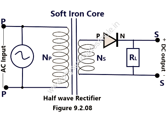
The AC supply is connected across the primary coil P of a step-down transformer. The secondary coil S of the transformer is connected to the junction diode and a low-resistance RL, as shown in Figure 9.2.08 as given above. The output DC voltage is obtained across the load resistance RL.
Working and Theory:
Let’s say the PN-junction diode becomes forward-biased during the first half of the input cycle. The traditional current will move in the arrowhead’s direction. In comparison to the lower end, the upper end of load resistance RL will have a positive potential. At any given time, the output across RL during the first half cycle will be inversely proportional to the current through RL. As a result, the amount of the forward bias will be proportional to the quantity of majority charge carriers crossing the junction, which in turn will depend on the current value of the AC input. Thus, the junction diode conducts for the first half of the input cycle.

Because the junction diode is reverse-biased during the second part of the cycle, there is no output across the load resistance RL. Due to the minority charge carriers, a little current will critically follow, and this half cycle will likewise yield a negligible output. The output is once again obtained during the subsequent half cycle as the junction diode is biased forward. Therefore, as illustrated in Figure 9.2.09, a half-wave rectifier produces a discontinuous and pulsating DC output across the load resistance. Therefore, half-wave rectification wastes a lot of energy and is not recommended.
Full Wave Rectifier:
A rectifier that rectifies both halves of each AC input cycle is called a full wave rectifier.
Principle:
It is based on the principle of valve action of a PN-junction diode. It will be conducted only when it is forward-biased. That means a PN-Junction diode offers no resistance path when it is forward-biased and high resistance when it is reverse-biased. When AC input is applied to the junction diode, it gets forward-biased during the first half cycle and reverse-biased during the next opposite half cycle. Thus, output is obtained during the alternate half cycle of the AC inputs.
Circuit arrangement:
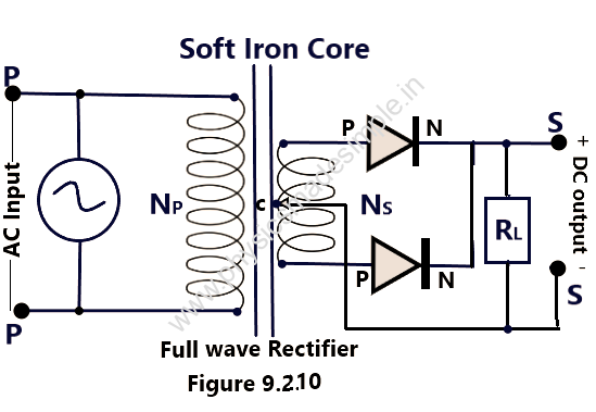
The AC supply is connected across the primary coil P of a step-down transformer. The two ends of the secondary coil S of the transformer are connected to the P-sections of the junction diodes D1 and D2. A load resistance RL is connected across the N-sections of the two diodes and the central tapping of the secondary coil, as shown in Figure 9.2.11. The output DC voltage is obtained across the load resistance RL.
Theory:
Assume that for the first half of the input cycle, coil S has a positive potential at its higher end and a negative potential at its lower end. While the diode D2 will become reverse biased, the PN-Junction diode D1 will become forward biased. The entire arrow will form the path along which the conventional current caused by the diode D1 will flow.
The situation will be exactly reversed when the input cycle’s second half arrives. The PN-Junction diode D2 will now conduct, and the regular current will flow in the direction of the dashed arrows. The output during both half cycles will be the same since the current during both half cycles flows from right to left through the load resistance RL. In relation to its left ends, the right end of the load distance RL will have a positive potential. The quantity of output overload resistance at any given time will fluctuate in line with the AC input, as stated in the context of the halfwave rectifier, as shown in Figure 9.2.011.
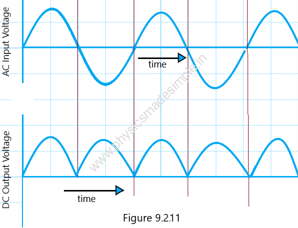
As a result, the output of a full-wave rectifier is continuous but pulsating. However, a filter circuit can be used to make it smooth.
Types of PN-Junction Diodes:
Depending on the types of working and structure of PN-Junction diodes, they have been classified into three various types. They have a wide range of applications in electronics. A few of them are discussed below.
Zener Diode:
When reverse-biased below its reverse breakdown voltage, a traditional junction barrier does not allow a significant current to flow. When the applied reverse voltage is very high in an ordinary PN-Junction diode, the valence electrons break free under the influence of the applied electric field and get accelerated enough to knock other electrons loose. As a result, there is a quick avalanche breakdown, and the diode conducts a significant amount of current in the opposite direction. This causes the diode to suffer long-lasting damage.
The specially designed junction diodes, which can operate in the reverse breakdown voltage region continuously without being damaged, are called Zener diodes.
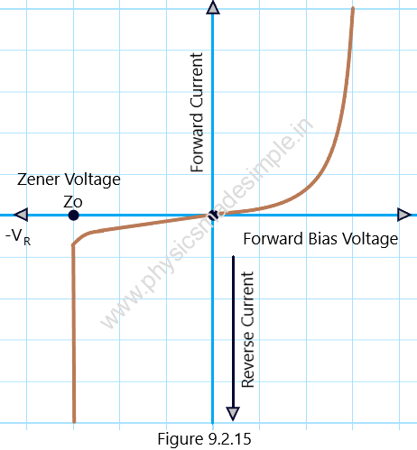
A Zener diode is built with a drastically lower breakdown voltage, or Zener voltage. The applied electric field affects how an avalanche breaks down. Thus, the Zener diode is created by altering the thickness of the junction layer to which the voltage is delivered.
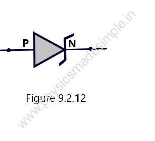
A Zener diode has a strongly doped PN-Junction diode that enables electrons to move from the P-type material’s Valence band to the N-type material’s conduction band. The voltage across a reverse-biased Zener diode will have a controlled breakdown and enable current to flow, maintaining the voltage at the Zener value. In the doping process, the breakdown voltage can be relatively precisely controlled. A Zener diode’s breakdown voltage can range from 4 V to several thousand volts. The sign in [Figure 9.2.12] stands for a Zener diode.
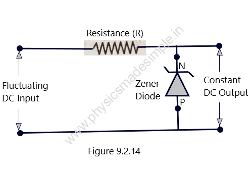
Zener diodes can be operated continuously in the breakdown zone without suffering damage. An outside resistance serves as a limiter for the current in this case. The voltage drop across them is independent of the current passing through them, which makes them special. Zener diodes are frequently employed to control the voltage present in a circuit. It is reverse-biased when linked in parallel to a source of variable voltage. When the voltage approaches the reverse breakdown voltage of a Zener diode, the diode begins to conduct. It then maintains the voltage at that level.
Zener diode as a Voltage regulator:
The Zener diode’s utility in supplying a constant voltage supply is depicted in the Figure. Based on the fact that in the reverse breakdown (the Zener) region, a very tiny change in the voltage across the Zener diode creates a very big change in the current flowing through the circuits, the Zener diode is used in this way. The resistance of the Zener diode decreases significantly if the voltage is raised above the Zener voltage.
Consider a situation where a falling resistor—say, a resistor R—is connected to a fluctuating DC supply, such as one from a rectifier, and the current flowing through the diode climbs out of proportion, increasing the voltage drop across the dropping resistor. The output voltage therefore returns to its initial level. Similar to how the current through a diode tends to decrease as the voltage across it tends to increase, the voltage drop across a dropping register decreases dramatically as a result, raising the voltage output to its usual level.
Photodiodes:
In semiconductors, electrons are released from the valence band, when energy is supplied to such electrons. This energy can be supplied in the form of heat or through an accelerating voltage. Light energy can also be used to produce the current inside the conductors.
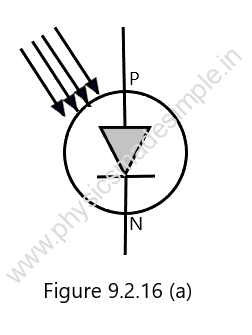

A junction diode made from light- or photo-sensitive semiconductor materials is called a photodiode. It is represented in terms of the symbol shown in Figure 9.2.16 (a).
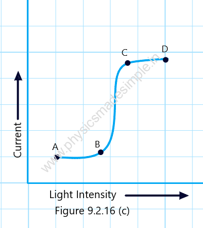
A specific current flows in the circuit if the photodiode is forward biased, as shown in [Figure 9.2.16(b)], as illustrated by portion AB of the graph in Figure 9.2.16(c). A dark current is defined as one that flows when no light is encountered. For as long as hv is greater than the forbidden gap energy, more electrons from the valence band go to the conduction band when photons of light with energy hv strike the photodiode. As a result, the circuit’s current rises. The photodiode is truly saturated as the light intensity rises since the current does not rise along with the increase in light intensity. The graph’s segment CD stands for the current at saturation.
Light Emitting Diodes (LEDs):
Light emitting diodes are electronic devices that convert electrical energy into light energy. The LEDs are just tiny light bulbs. But unlike ordinary incandescent bulbs, they do not have a filament that will burn out. Further, they do not get hot during their use. These devices have the advantages of small size, energy savings, long life, and bright colors. On account of these special characteristics, LEDs are widely used in various fields, ranging from the daily needs of lightning sources to high definition display systems and optical communications.
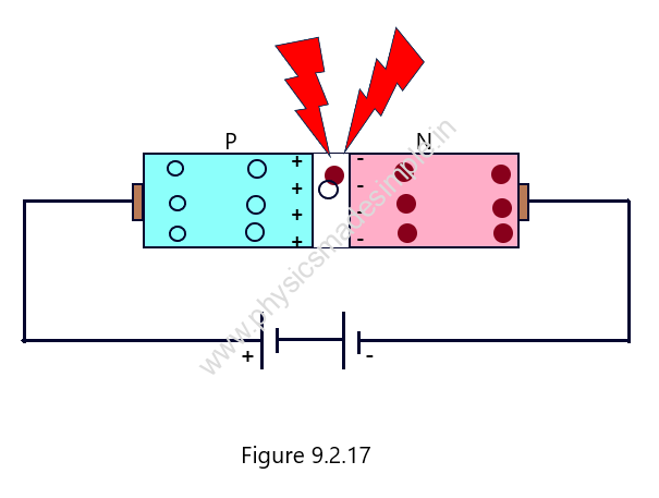

When forward-biased, junction diodes all produce some visible light. Since the energy is released in the infrared spectrum in silicon and germanium diodes, it cannot stimulate eyesight. While gallium arsenide phosphide (GaAsP) junction diodes produce radiation in the visible range, gallium arsenide (GAAs) junction diodes release energy in the infrared spectrum. A junction diode like this is referred to as an LED.
The PN Junction is an LED’s most crucial component. Between the P and N regions, the Junction serves as a barrier to the flow of electrons. The electrons don’t pass the junction into the P region and create a current via the LED until enough voltage is provided. It should be noted that the resistance used to control the current in LEDs is incredibly low. To prevent any harm to the LED, a register must be used in series with it, as illustrated in [Figure 9.2.16 (b)].
The LED electrons cross the junction and enter the P region when a sufficient voltage is provided. The electrons are drawn to the positive holes as soon as they reach the P region. In the P region, an electron can recombine if it gets close enough to the hole. Electric potential is transformed into electromagnetic energy each time an electron recombines with a positive hole, and a photon of light with a frequency specific to the semiconductor material is released. 1.90 eV is the forbidden energy gap in GaAsP. It is possible to determine the electromagnetic radiation’s wavelength by
𝛌 = (hc/Eg)
= (6.62 x 10-34 x3 x 108/1.90 x 1.6 x 10-19) = 6500 Ao
The energy band topologies produced by various semiconductor materials and dopants can alter the color of the light emitted by LEDs. Light-emitting diodes manufactured of gallium nitride can emit light in a variety of colors, including blue, green, and purple, but LEDs made of gallium arsenide emit red light as an example of an acceptable citation. LEDs are able to cover a wide spectral range thanks to their material versatility.
Key Points:
Pentavalent materials are used as dopants to produce N-type semiconductors, while trivalent materials are used as dopants to produce P-type semiconductors.
N-type semiconductors have a large number of electrons, and P-type semiconductors have a large number of holes. But both types of crystals are electrically neutral.

