Logic gates
Logic gates are the building blocks of digital electronics. They are used in digital electronics to change one voltage level (the input voltage) into another (the output voltage) according to some logical statement relating them.
We’ve focused on analog electronic circuits so far. These circuits use continuous or analog voltage signals, which are voltage signals that change continuously throughout time. A typical voltage signal with sinusoidal 0–5 V variation is shown in Fig. 9.3.01 (b)
The electronic circuits used in digital technology use logic gates that utilize totally distinct voltage signals. As opposed to analog voltage signals, which change continuously over time, these signals have pulse waves. Instead, such a signal only has two voltage levels, which are either zero or some fixed voltage value. These are digital voltage signals. A digital voltage signal that will always be either 0 V or 5 V at any constant is shown in Fig. 9.3.01 (a)
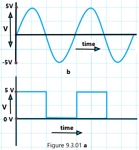
The development of digital electronics relies on logic gates, which in turn rely on the binary representation of these two voltage levels as the numbers 0 and 1. The results of digital electronics are the counters composed of the logic gates on the computerette. Now that we have a basic understanding of the binary number system, we will move on to the logic gates, which are the fundamental components of digital electronics.
BINARY NUMBER SYSTEM
Only the digits 0 and 1 are used in the binary number system, which is a type of code which is the basis of Logic Gates
The number next to 1 in the binary number system (0,1) is obtained by writing the second digit (i.e., 1) followed by the first (i.e., 0), and it is called 10. This is analogous to how the number next to 9 in the decimal number system (0, 1, 2, 3, 5, 6, 7, 8, and 9) is obtained by writing the second digit (i.e., 1) followed by the first (i.e., 0), and it is called 9. Thus, the binary equivalent of the decimal numeral 2 is 10. In a similar way, the binary equivalent of the decimal numeral 3 is 11, and so on.
The binary representation of any decimal digit or number can be easily obtained using the double-dabble method.
Double dabbed method: To represent a decimal number in the binary number system using the double dabbed method, the following steps are involved:
Step 1. Go on dividing the given decimal number by 2 until the quotient is zero.
Step 2. Then, the remainders taken in reverse order (obtained in successive divisions) give the binary representation of the given decimal number.
For Examples:
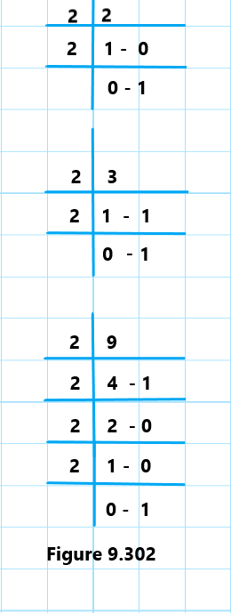
To find the binary representation of the decimal number 2,
(1) The remainders in reverse order are 1 and 0. (2) Therefore, the binary representation of the decimal number 2 is 10.
To find the binary representation of the decimal number 3,
(1) The remainder, in reverse order, are 1 and 1.
(2) Therefore, the binary representation of the decimal number 3 is 11.
To find the binary representation of the decimal number 9,
(1) The remainder in reverse order are 1, 0, and 1.
(2) Hence, the binary representation of the decimal number 9 is 1001.
Similarly, the binary representation of the decimal number 37 is 100101.
The Following points are very important to note about the binary number system, as they are the basis of the operation of the logic gates in digital electronics:
1. Each digit of a binary number is called a bit.
2. The first digit is called the least significant bit (LSB), while the Last digit is called the most significant bit (MSB). For example, in the binary number 110, 0 is LSB and 1 is MSB.
3. The binary representation of the decimal, 37, was found to be 100101. The decimal number 37 is represented as (37)10, and its binary representation is (100101)2. Thus,
(37)10=(100101)2
4. In the decimal number system, the multiplier of a digit in unit place is 10, the multiplier of a digit in tenth place is 101, the multiplier of a digit in hundredth place is 102, and so on. In the binary number system, the base is 2. Therefore, in a binary number system, the multipliers of the bits are 20, 21, 22,… starting from LSB until MSB is reached. With the help of these multipliers, the decimal representation of a binary number can be easily found, as explained in the following two examples:
To find the decimal representation of the binary number 110:
( 1MSB 1 0LSB )2 = 1×2²+1×2¹+0×2¹×2⁰
= 4+2+0 =6
Thus, decimal representation of binary number 110 is 6
To find the decimal representation of the binary number 10100:
( 1MSB 0 1 0 0LSB )2 =1×2⁴+0×2³+1×2²+0×2¹×2⁰
=16+0+4+0+0=20
Thus, the decimal representation of the binary number 10100 is 20.
Logic Gates:
The foundational elements of digital electronics are logic gates. According to a logical relationship between them, they are employed in digital electronics to convert one voltage level (input voltage) into another (output voltage).
Thus, logic gates is a digital circuit, which works according to some logical relationship between input and output voltages.The logic gates have only one output, but they may have one or more inputs. A table known as a truth table or table of combinations serves as an expression of the relationship between the potential values of input and output voltage. The truth tables of the logic gates are the tables that show all the input and output possibilities for the logic gates.
Based on the binary character of logic, George Boole created a new type of algebra. There are just two possible outcomes for a logical assertion, such as HIGH or LOW, ON or OFF, CLOSED or OPEN, YES or NO, TRUE or FALSE, etc. The binary numerals 1 and 0 represent these two logical claims. The HIGH value is represented by the binary number 1, and the LOW value is represented by the binary number 0.
Boolean expressions are the logical formulas that logic gates employ.
The OR gate, AND gate, and NOT gate are the three fundamental logic gates used in digital electronics. They adhere to the following Boolean expression:
1. In Boolean algebra, the addition sign (+) is referred to as OR. The Boolean expression:
y = A+B… (3.11)
is read as y equals A OR B.
The OR gate is designed on the basis of a Boolean expression (3.01).
The multiplication sign (.) Is referred to as AND in Boolean algebra. The Boolean expression:
y = A . B (3.12)
is read as y equals A AND B
The AND gate is designed on the basis of a Boolean expression (3.02).
The bar sign (-) is referred to as NOT in Boolean algebra. The Boolean expression:

is read as y equal NOT A.
The NOT operation is also called negation or inversion. The NOT gate is designed on the basis of a Boolean expression (3.03).
Before taking up the study of logic gates, it is worthwhile to understand the switching action of a transistor
OR Gate
The OR gate is one of the logic gates that has two inputs and one output logic state. It combines both inputs A and B with the output y following the Boolean expression
Y = A + B
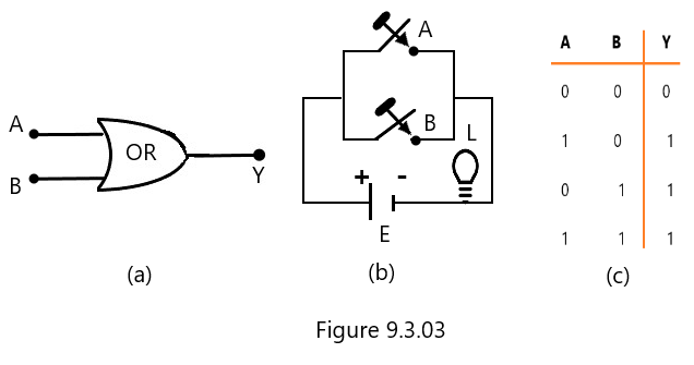
It is read as Y equals A or B. The OR gate is represented as shown in Figure 9.3.03 (a). The various possible combinations of the inputs and outputs of the OR gate can be easily understood with the help of the electrical circuit shown in Figure 9.3.03 (b). In this electrical circuit, a parallel combination of two switches A and B is connected to a battery and a lamp L.
The operation of the electrical circuit mentioned above makes it simple to reach the following conclusions:
1. If switches A and B are both OFF (i.e., A = 0, B = 0), the lamp won’t light up (i.e., y = 0).
2. The light will glow (i.e., y = 1) if switch A is closed and switch B is open (i.e., A = 1 and B = 0).
3. The lamp will glow (i.e., y = 1) if switch A is OPEN and switch B is CLOSED (i.e., A = 0 and B = 1).
4. The bulb will glow (i.e., =1) if both switches are closed (A = 1, B = 1).
As a result, even when either switch A or switch B is closed in the electrical circuit, the lamp continues to shine (or an output is produced). The electrical circuit seen in Figure 9.3.03 (b) is known as the OR gate for this reason. For the electrical circuit in question, an OR gate, there are several conceivable input-output combinations that can be expressed in the form of Table 9.3.03 (c). The OR gate’s truth table is known as the Truth Table of the OR Gate.
As shown in Fig. 9.3.04, an electronic circuit utilizing two diodes, D1 and D2, is used to implement the OR gate in practice. As described below, the two diodes serve as switches A and B.
Either 0V or 5V can be used as the input voltage at A OR B.
The following scenarios are potential:
(a) A and B are both 0. Since neither of the diodes D1 nor D2 conduct when the inputs A and B are connected to earth at 0 V, there is no voltage across the resistor and no output Y as a result.
(b) If B = 0, then A = 1. The junction diode D1 conducts when input A is connected to the positive terminal of the battery (5 V) and input B is connected to the ground (0 V); however, diode D2 does not conduct when input A is connected to the negative terminal of the battery (reverse biased). If the diodes are perfect, output Y (as a result of diode D1’s conduction) will also be 5 V or 1. In a binary system, a voltage at a high level is represented as 1.
(c) A = 0 and B = 1. In this case, the reverse of what happened above will happen, i.e., the diode D1 will not conduct and D2 will conduct. Obviously, the output will again be 5 V or 1.

Since input-output combinations of the electronic circuit shown in Fig. 9.3.04 are the same as those of the electric circuit shown in Fig. 9.3.03 (b), and Table 9.3.03 (c) also represents the truth table of the OR gate, which is realized with the help of the electronic circuit shown in Fig. 9.3.04
The AND gate
The AND gate is also one of the logic gates, having two inputs and one output. It combines the inputs A and B with the output y according to the following Boolean expression:
y = A. B
It is read as y equals A AND B. The AND logic gates are represented as per the symbol shown in Figure 9.3.05 (a).
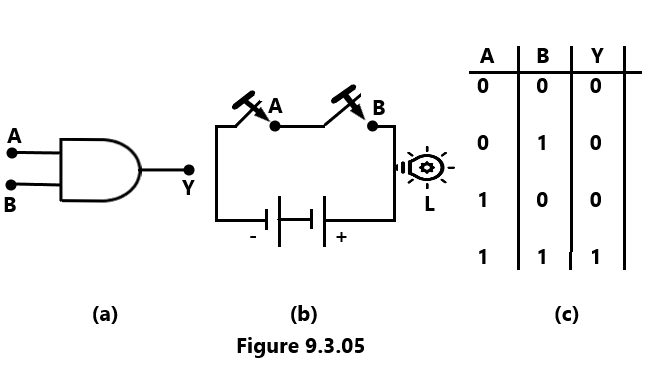
The electrical circuit depicted in Figure 9.3.05 (b) makes it simple to find the many different combinations of the inputs and outputs of the AND gate. Here, a battery and a lamp L are linked in series with switches A and B. The findings listed below are simple to draw from the workings of the above electrical circuit:
(A) The bulb won’t light up (i.e., y = 0) if both switches A and B are OPEN (i.e., A = 0, B = 0).
(b) The bulb won’t light up (i.e., y = 0) if switch A is CLOSED and switch B is OPEN (i.e., A = 1, B = 0).
(c) The bulb won’t glow (i.e., y = 0) if switch A is OPEN and switch B is CLOSED (i.e., A = 0, B = 1).
(d) Only the lamp will glow if both switches A and B are CLOSED (A = 1 and B = 1) (y = 1).
It follows that the lamp will only light up (or provide an output) in the electrical circuit shown when both switches are closed, i.e., when switches A and B are closed. This is why the electrical circuit in Fig. 9.3.05 (b) is necessary for the AND logic gates. Table 3.02 can be used to represent the many input-output configurations for the electric circuit, or AND gate, in question. This is known as the truth table of the AND gate.
The AND logic gates can be realized by the electronic circuit by making use of two ideal semiconductor junction diodes, D1 and D2, as shown in Fig. 9.3.06 The resistor R is connected to the positive terminal of a 5 V battery. The operation of the AND logic gates can be discussed in the following four cases:
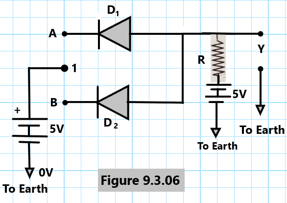
(a) When A = B = 0, The diodes D1 and D2 will conduct as they are forward-biased. The voltage drop between D1 and D2 will be the output, Y. Since the PN-Junction diodes are assumed to be ideal, there is no voltage drop across them. As a result, the output y is 0
(b) When A =1 and B =0, The diodes D2 in this case will conduct, and diode D1 will remain idle. Now, the output Y is the voltage across D2, and hence it is 0.
(c) When A =0 and B =1, The diode D1, in this case, will conduct, while D2 will not conduct. Now, output y is the voltage across D1, which is 0.
(d) when A = 1 and B = 1: In this case, both diodes will not conduct as they are reverse-biased. The output Y will be equal to the battery voltage of 5 V, i.e., equal to 1.
Obviously, Table 9.3.05 (b) represents the truth table of the AND logic gates realized with the electronic circuit as shown in Figure 9.3.06.
The nOT logic gates
The NOT logic gates have one input and one output logic state. They relate the input A to the output Y following the Boolean expression.

The above Boolean expression of NOT gate is read as Y NOT equals A. The way the NOT gate gives the output is why it is also called an invertor gate. It is represented in terms of the symbol shown in Fig. 3.09 (a).
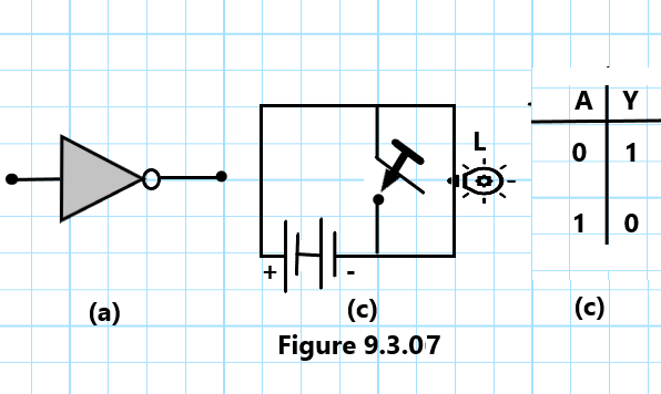
It is clear that the lamp glows (or output is obtained) in the given electrical circuit when switch A is kept open. On account of this reason, the electrical circuit shown in Figure 9.3.07 (b) is called the NOT gate. The two possible input-output combinations can be written in the form of Table (c). It is called the truth table of the NOT gate.
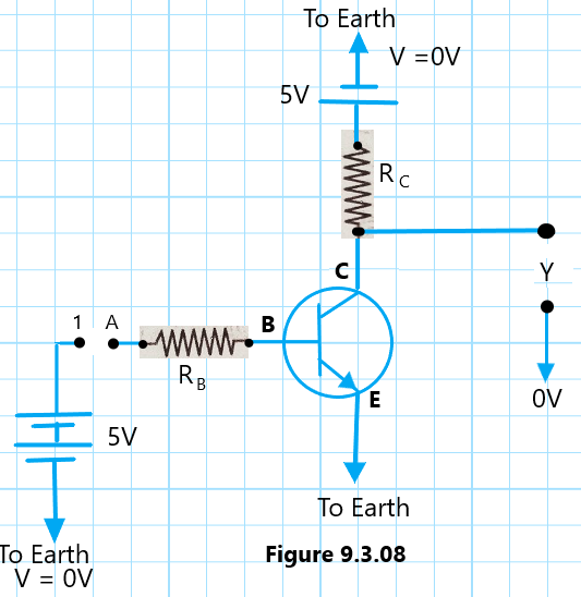
The NOT gate in digital electronics can be realized using transistors, as shown in [Figure 9.3.08]. The base (B) of the transistor is connected to A through a resistor RB, while the emitter (E) is earthed. The collector is earthed through a resistor Rc and a 5 V battery. The operation of the NOT gate can be understood and discussed in the following two cases:
(a) When A = 0, the base of the transistor is equivalent to being connected to the earth. Therefore, the base-emitter junction is not forward-biased. The base current and the collector current are both zero. The transistor is said to be in cut-off mode. The output Y will be equal to the voltage of the battery connected to the collector, i.e., 5 V. In other words, when A is 0, Y will be 1.
(b) When A = 1, the base-emitter junction gets forward biased, which leads to a large collector current flowing in the circuit. The transistor is said to have gone to Saturation. The voltage drop, as per Ohm’s law, across the resistor Rc is just equal to 5 V, and the output Y is very nearly 0.
Obviously, Table 9.3.07 (c) represents the truth table of the NOT logic gates achieved by making use of the electronic circuit shown in in[Figure 9.3.08]
Combination Of Logic Gates
The three basic logic gates, i.e., OR, AND, and NOT, can be combined to give rise to complicated digital circuits. We now discuss a few combinations of these basis gates using their symbols:
1. The NAND logic gates
These are the logic circuits in which an AND gate is connected to a NOT gate. If the output (y*) of AND logic gates is connected to the input of a NOT gate [Figure 9.3.09(a)], the logic gates so obtained are called NAND logic gates. The logic symbol of the NAND gate is shown in Figure 9.3.09(b).

The truth table of the NAND gate can be obtained from the combination of the truth tables of the AND and NOT gates. It will be as given in table 9.3.09 (c).
The Boolean expression for the NAND gate is

2. The NOR gate
These are the logic circuits in which an OR gate is connected to a NOT gate. If the output (y*) of OR logic gates is connected to the input of a NOT gate [Figure 9.3.09(a)], the logic gates so obtained are called NOR logic gates. The logic symbol of the NAND gate is shown in Figure 9.3.09(b).
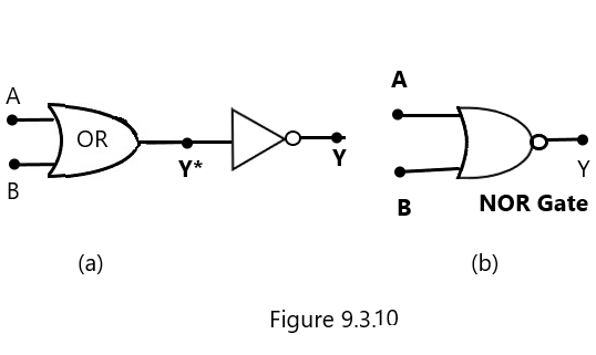
The truth table of NOR gate can be obtained from the combination of the truth tables of OR and NOT gates and is given in tables 9.3.11 (a) and (b)
| A | B | Y* | Y |
| 0 | 0 | 0 | 1 |
| 1 | 0 | 1 | 0 |
| 0 | 1 | 1 | 0 |
| 1 | 1 | 1 | 0 |
| A | B | Y |
| 0 | 0 | 1 |
| 1 | 0 | 0 |
| 0 | 1 | 0 |
| 1 | 1 | 0 |
Boolean expression for the NOR gate is

The NAND Gate—Building Block In Digital Circuits
The different gates can be obtained through the repeated use of the three basic gates, i.e., the OR, AND, and NOT gates. The repeated use of the NAND gate can produce all three basic gates. Thus, in digital circuits, the NAND gate serves as a building block. Now, we proceed to show how the repeated use of the NAND gate can produce OR, AND, and NOT gates.
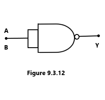
1. To produce a NOT gate by using a NAND gate Suppose that the two inputs of the NAND gate are joined so that it has one input [Fig. 3.13].
| A | B | Y |
| 0 | 0 | 1 |
| 1 | 1 | 0 |
Setting B =A in the truth table of the NAND gate, we obtain the truth table as given in table 3.06. Since it is the truth table of the NOT gate, it follows that a NAND gate functions as the NOT gate when it’s two inputs are joined.
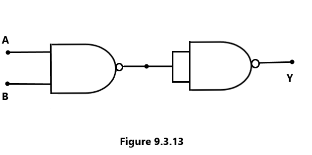
2. To produce an AND gate by using a NAND gate:
Suppose that the output of the NAND gate is connected to the NOT gate (obtained from the NAND gate) when it’s two inputs are joined, as shown in Figure 9.3.13
| A | B | Y* | Y |
| 0 | 0 | 1 | 0 |
| 1 | 0 | 1 | 0 |
| 0 | 1 | 1 | 0 |
| 1 | 1 | 0 | 1 |
The truth table of the combination of a NAND and a NOT gate will be obtained as shown in the table given above. It follows that it is the truth table (read columns A, B, and Y only) of the AND gate. Hence, a NAND gate functions as the AND gate when it is connected to a NOT gate (from the NAND gate).
To produce OR gate by using NAND gates
Let us suppose that the inputs A and B are connected to the two NOT gates (obtained from the NAND gates) individually. The inputs A and B will get inverted, i.e., will appear as A bars and B bars. These inputs are then fed to the NAND gate, as shown in Figure 9.3.14.

| A | B | Ā | Ḃ | Y |
| 0 | 0 | 1 | 1 | 0 |
| 0 | 1 | 1 | 0 | 1 |
| 1 | 0 | 0 | 1 | 1 |
| 1 | 1 | 0 | 0 | 1 |
The truth table of the arrangement will be as shown in Table 9.314. It follows that it is the truth table of the OR gate (read columns A, B, and Y only). Hence, if the inputs A and B, after being inverted by using two NOT gates (obtained from the NAND gates), are then fed to the NAND gate, the arrangement functions as the OR gate.
THE XOR GATE
An XOR gate is obtained using OR, AND, and NOT logic gates, as shown in Figure 9.3.15(a). It is also called an exclusive OR gate, and its logic symbol is as shown in Figure 9.3.15 (b).

At the first stage, the inputs A and B will get inverted due to the two NOT gates, i.e., they will appear as Ā and Ḃ
At the second stage, the inputs for two AND gates will be Ā, B, and A, Ḃ, respectively, as shown in Figure 9.3.15 (a). The outputs of the two gates will be y and y’. The outputs of the AND gates will be 1 when both inputs are 1.
At the third stage, y and y’ will form the inputs for the OR gate. The output of OR gate will be 1, when either or both the inputs are 1
| A | B | Ā | Y* | Y** | Y | |
| 0 | 0 | 1 | 1 | 0 | 0 | 0 |
| 0 | 1 | 1 | 0 | 1 | 0 | 1 |
| 1 | 0 | 0 | 1 | 0 | 1 | 1 |
| 1 | 1 | 0 | 0 | 0 | 0 | 0 |
| A | B | Y | |
| 0 | 0 | 0 | |
| 0 | 1 | 1 | |
| 1 | 0 | 1 | |
| 1 | 1 | 0 |
The above facts have been used to write the truth table for the whole arrangement as given in Table 3.09 (a), which is equivalent to the final truth table given in Table 3.09 (b).


